

| CAD Model: | View CAD Model |
| Pkg. Type: | VFQFPN |
| Pkg. Code: | NLG72 |
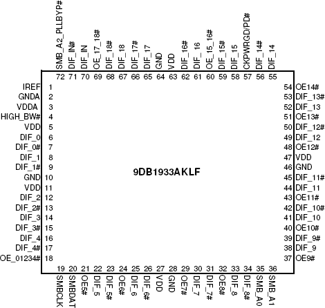
| Lead Count (#): | 72 |
| Pkg. Dimensions (mm): | 10.0 x 10.0 x 1.0 |
| Pitch (mm): | 0.5 |
| Moisture Sensitivity Level (MSL) | 3 |
| Pb (Lead) Free | Yes |
| ECCN (US) | EAR99 |
| HTS (US) | 8542.39.0090 |
| Lead Count (#) | 72 |
| Carrier Type | Tray |
| Moisture Sensitivity Level (MSL) | 3 |
| Qty. per Reel (#) | 0 |
| Qty. per Carrier (#) | 168 |
| Pb (Lead) Free | Yes |
| Pb Free Category | e3 Sn |
| Temp. Range (°C) | 0 to 70°C |
| Accepts Spread Spec Input | Yes |
| Advanced Features | HW PLL mode control, Multiple SMBus addresses |
| App Jitter Compliance | PCIe Gen1, PCIe Gen2, PCIe Gen3 |
| Architecture | Common |
| C-C Jitter Max P-P (ps) | 50 |
| C-C Jitter Typ P-P (ps) | 25 |
| Core Voltage (V) | 3.3 |
| Diff. Input Signaling | HCSL |
| Diff. Inputs | 1 |
| Diff. Output Signaling | HCSL |
| Diff. Outputs | 19 |
| Diff. Termination Resistors | 76 |
| Feedback Input | No |
| Function | Zero Delay Buffer |
| Input Freq (MHz) | 100 |
| Input Type | HCSL |
| Inputs (#) | 1 |
| Length (mm) | 10 |
| MOQ | 168 |
| Output Banks (#) | 1 |
| Output Freq Range (MHz) | 10 - 167 |
| Output Skew (ps) | 150 |
| Output Type | HCSL |
| Output Voltage (V) | 3.3 |
| Outputs (#) | 19 |
| PLL | Yes |
| Package Area (mm²) | 100 |
| Phase Jitter Max RMS (ps) | 1 |
| Phase Jitter Typ RMS (ps) | 0.6 |
| Pitch (mm) | 0.5 |
| Pkg. Dimensions (mm) | 10.0 x 10.0 x 1.0 |
| Pkg. Type | VFQFPN |
| Power Consumption Typ (mW) | 1515 |
| Prog. Clock | No |
| Prog. Interface | SMBUS |
| Published | No |
| Requires Terms and Conditions | Does not require acceptance of Terms and Conditions |
| Supply Voltage (V) | 3.3 - 3.3 |
| Tape & Reel | No |
| Thickness (mm) | 1 |
| Width (mm) | 10 |
The 9DB1933 zero-delay buffer supports PCIe Gen3 requirements, while being backwards compatible to PCIe Gen2 and Gen1. The 9DB1933 is driven by a differential SRC output pair from an IDT 932S421, 932SQ420, or equivalent, main clock generator. It attenuates jitter on the input clock and has a selectable PLL bandwidth to maximize performance in systems with or without Spread-Spectrum clocking.