
| CAD Model: | View CAD Model |
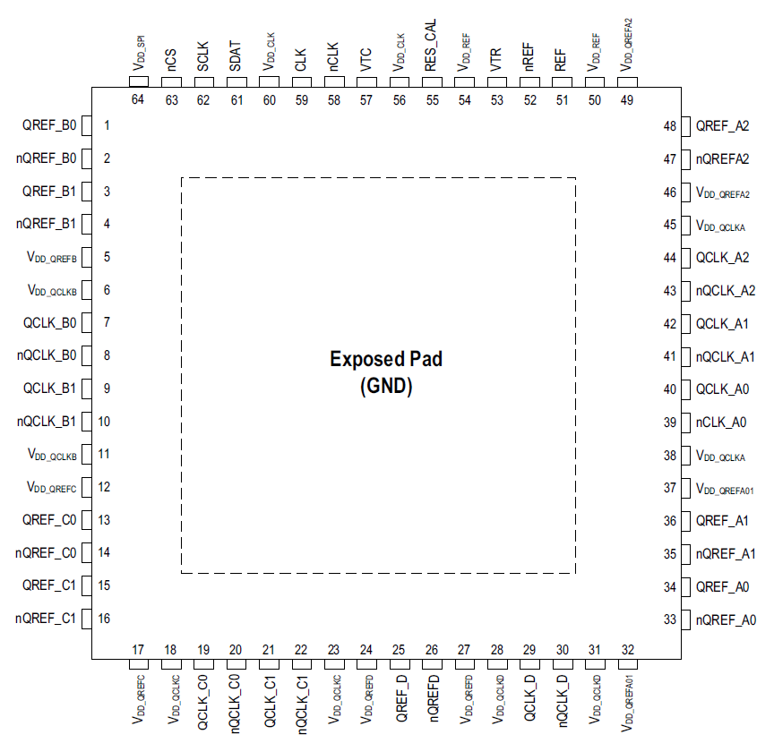
| Pkg. Type: | VFQFPN |
| Pkg. Code: | NLG64 |
| Lead Count (#): | 64 |
| Pkg. Dimensions (mm): | 9.0 x 9.0 x 0.9 |
| Pitch (mm): | 0.5 |
| Moisture Sensitivity Level (MSL) | 3 |
| Pb (Lead) Free | Yes |
| ECCN (US) | EAR99 |
| HTS (US) | 8542.39.0090 |
| Lead Count (#) | 64 |
| Carrier Type | Tray |
| Moisture Sensitivity Level (MSL) | 3 |
| Qty. per Reel (#) | 0 |
| Qty. per Carrier (#) | 207 |
| Pb (Lead) Free | Yes |
| Pb Free Category | e3 Sn |
| Temp. Range (°C) | -40 to 85°C (Tc ≤ 105°C) |
| Country of Assembly | CHINA |
| Country of Wafer Fabrication | SINGAPORE |
| 105°C Max. Case Temp. | 1 |
| Adjustable Phase | Yes |
| Advanced Features | JESD204B, Dual Buffer, Individual output bank enable, Individual output enable, Per-bank divider, Universal outputs |
| Channels (#) | 2 |
| Core Voltage (V) | 3.3 |
| Divider Value | 1, 2, 4, 8, 12, 16 |
| Function | Buffer, Divider |
| Input Freq (MHz) | 3000 |
| Input Type | LVPECL, LVDS |
| Inputs (#) | 2 |
| Length (mm) | 9 |
| Longevity | 2040 Apr |
| MOQ | 207 |
| Noise Floor (dBc/Hz) | -158.8 |
| Output Banks (#) | 4 |
| Output Freq Range (MHz) | 3000 |
| Output Skew (ps) | 100 |
| Output Type | LVPECL, LVDS |
| Output Voltage (V) | 3.3 |
| Outputs (#) | 16 |
| Package Area (mm²) | 81 |
| Pitch (mm) | 0.5 |
| Pkg. Dimensions (mm) | 9.0 x 9.0 x 0.9 |
| Pkg. Type | VFQFPN |
| Price (USD) | $11.7713 |
| Published | No |
| Requires Terms and Conditions | Requires acceptance of Terms and Conditions |
| Supply Voltage (V) | 3.3 - 3.3 |
| Tape & Reel | No |
| Thickness (mm) | 0.9 |
| Width (mm) | 9 |
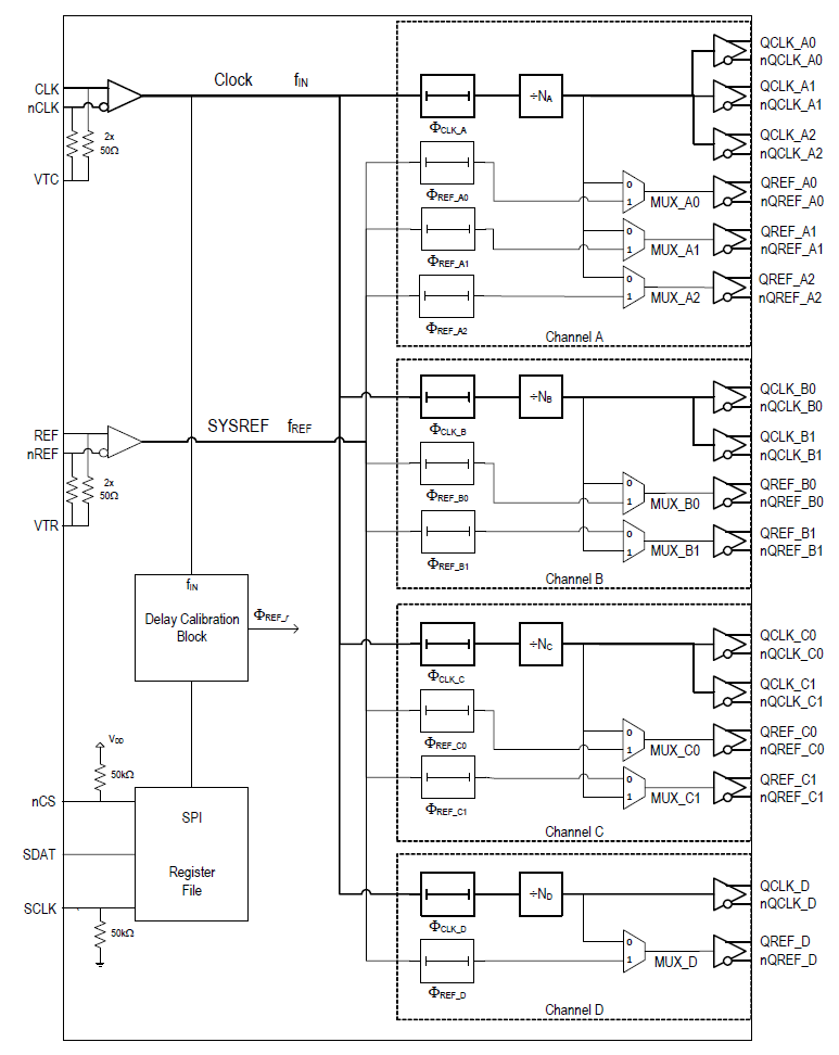
The 8V79S680 is a fully integrated, clock and SYSREF signal fanout buffer for JESD204B applications. It is designed as a high-performance clock and converter synchronization solution for wireless base station radio equipment boards with JESD204B subclass 0, 1, and 2 compliance. The main function of the device is the distribution and fanout of high-frequency clocks and low-frequency system reference signals generated by a JESB204B clock generator such as the 8V19N480, extending its fanout capabilities and providing additional phase delay. The 8V79S680 is optimized to deliver very low phase noise clocks and precise, phase-adjustable SYSREF synchronization signals as required in GSM, WCDMA, LTE, and LTE-A radio board implementations. Low-skew outputs, low device-to-device skew characteristics, and fast output rise/fall times help the system design to achieve deterministic clock and SYSREF phase relationships across devices.
The device distributes the input clock and JESD204B SYSREF signals to four fanout channels. In each channel, both input clock and SYSREF signals are fanned out to multiple clock (QCLK) and SYSREF (QREF) outputs. Clock signals can be frequency-divided in each channel. Configurable phase-delay circuits are available for both clock and SYSREF signals. The propagation delays in all signal paths are fully deterministic to support fixed phase relationships between clock and SYSREF signals within one device. The clock divider can be bypassed for low-latency clock paths. The device facilitates synchronization between frequency dividers within the device and across multiple devices, removing phase ambiguity introduced in dividers between power and configuration cycles.
Each channel supports clock frequencies up to 3GHz. In an alternative configuration, for instance, JESD204B subclass 0 and 2, the SYSREF (QREF) outputs can be configured as regular clock outputs adding additional clock fanout to the device.
All outputs are very flexible in amplitude configuration and output signal termination and allow both DC and AC coupling. Outputs can be disabled and powered down when not used. The SYSREF output pre-bias feature supports the prevention of power-on glitches and enables AC-coupling of the system synchronization signals.
The 8V79S680 is configured through a 3-wire SPI serial interface. The device is packaged in a lead-free (RoHS 6) 64-lead VFQFN package. The extended temperature range supports wireless infrastructure, telecommunication, and networking end equipment requirements.