

| CAD Model: | View CAD Model |
| Pkg. Type: | VFQFPN |
| Pkg. Code: | NLG88 |
| Lead Count (#): | 88 |
| Pkg. Dimensions (mm): | 10.0 x 10.0 x 0.9 |
| Pitch (mm): | 0.4 |
| Moisture Sensitivity Level (MSL) | 3 |
| Pb (Lead) Free | Yes |
| ECCN (US) | EAR99 |
| HTS (US) | 8542.39.0090 |
| Lead Count (#) | 88 |
| Carrier Type | Tray |
| Moisture Sensitivity Level (MSL) | 3 |
| Pkg. Dimensions (mm) | 10.0 x 10.0 x 0.9 |
| Qty. per Reel (#) | 0 |
| Qty. per Carrier (#) | 168 |
| Pb (Lead) Free | Yes |
| Pb Free Category | e3 Sn |
| Temp. Range (°C) | -40 to 85°C |
| Accepts Spread Spec Input | No |
| Adjustable Phase | Yes |
| Advanced Features | Holdover, Phase Delay, Input Switching, JESD204B, Programmable Clock |
| Channels (#) | 1 |
| Core Voltage (V) | 3.3V |
| Country of Assembly | TAIWAN, CHINA |
| Country of Wafer Fabrication | SINGAPORE, UNITED STATES |
| DPLL Channels (#) | 0 |
| Feedback Divider Resolution (bits) | 12 |
| Fractional Output Dividers (#) | 0 |
| Frequency Plan | 3932.16 / Output_Divider |
| Input Freq (MHz) | 30.72 - 2000 |
| Input Redundancy | Input Monitor, Auto-switch, Manual switch, Revertive and non-revertive switch, Holdover |
| Input Ref. Divider Resolution (bits) | 12 |
| Input Type | LVDS, LVPECL |
| Inputs (#) | 2 |
| JESD204B/C Compliant | Yes |
| Length (mm) | 10 |
| Loop Bandwidth Range (Hz) | 20 - 100 |
| MOQ | 168 |
| Noise Floor (dBc/Hz) | -160.2 |
| Output Banks (#) | 5 |
| Output Divider Resolution (bits) | 8 |
| Output Freq Range (MHz) | 19.6608 - 3932.16 |
| Output Skew (ps) | 100 |
| Output Type | LVDS, LVPECL |
| Output Voltage (V) | 3.3V |
| Outputs (#) | 15 |
| PLL | Yes |
| Package Area (mm²) | 64 |
| Phase Jitter Typ RMS (fs) | 46 |
| Phase Jitter Typ RMS (ps) | 0.046 |
| Phase Noise Supports GSM | Yes |
| Pitch (mm) | 0.4 |
| Pkg. Type | VFQFPN |
| Ports (#) | 1 |
| Price (USD) | $14.99958 |
| Product Category | JESD204B/C |
| Prog. Clock | Yes |
| Published | No |
| Supply Voltage (V) | 3.3 - 3.3 |
| Synthesis Mode | Integer |
| Tape & Reel | No |
| Thickness (mm) | 0.9 |
| Width (mm) | 10 |
| Xtal Freq (KHz) | 30720 - 500000 |
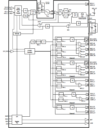
The 8V19N492-39 is a fully integrated FemtoClock™ NG jitter attenuator and clock synthesizer that is designed as a high-performance clock solution for conditioning and frequency/phase management of wireless base station radio equipment boards. The device is optimized to deliver excellent phase noise performance as required in GSM, WCDMA, LTE, LTE-A, and 5G radio board implementations.
The device supports JESD204B/C subclass 0 and 1 clocks. A two-stage PLL architecture supports both jitter attenuation and frequency multiplication. The first stage PLL is the jitter attenuator and uses an external VCXO for best possible phase noise characteristics. The second stage PLL locks on the VCXO-PLL output signal and synthesizes the target frequency.
The 8V19N492-39 supports the clock generation of high-frequency clocks from the selected VCO and low-frequency synchronization signals (SYSREF). SYSREF signals are internally synchronized to the clock signals. Delay functions exist for achieving alignment and controlled phase delay between system reference and clock signals and to align/delay individual output signals. The two redundant inputs are monitored for activity. Four selectable clock switching modes are provided to handle clock input failure scenarios. Auto-lock, individually programmable output frequency dividers, and phase adjustment capabilities are added for flexibility. The device is configured through a selectable 3/4-wire SPI interface and reports lock and signal loss status in internal registers and via a lock detect (LOCK) output. Internal status bit changes can also be reported via the nINT output. The 8V19N492-39 is ideal for driving converter circuits in wireless infrastructure, radar/imaging, and instrumentation/medical applications.
For information regarding evaluation boards and material, contact your local sales representative.