
| CAD Model: | View CAD Model |
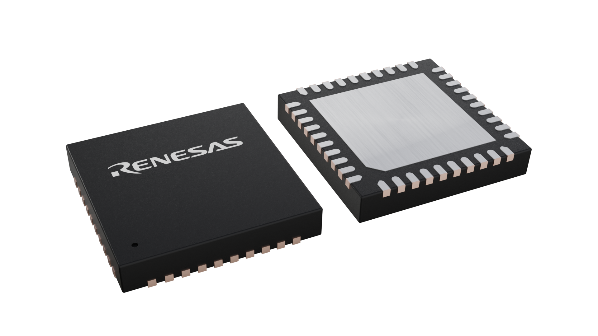
| Pkg. Type: | VFQFPN |
| Pkg. Code: | NLG40 |
| Lead Count (#): | 40 |
| Pkg. Dimensions (mm): | 6.0 x 6.0 x 0.9 |
| Pitch (mm): | 0.5 |
| Moisture Sensitivity Level (MSL) | 3 |
| Pb (Lead) Free | Yes |
| ECCN (US) | EAR99 |
| HTS (US) | 8542.39.0090 |
| Pkg. Type | VFQFPN |
| Lead Count (#) | 40 |
| Carrier Type | Reel |
| Moisture Sensitivity Level (MSL) | 3 |
| Qty. per Reel (#) | 5000 |
| Qty. per Carrier (#) | 0 |
| Pb (Lead) Free | Yes |
| Pb Free Category | e3 Sn |
| Temp. Range (°C) | -40 to 85°C |
| Additive Phase Jitter Typ RMS (fs) | 50 |
| Adjustable Phase | No |
| Advanced Features | Individual OE control |
| Channels (#) | 1 |
| Input Freq (MHz) | 2000 |
| Inputs (#) | 2 |
| Length (mm) | 6 |
| Longevity | 2040 Apr |
| MOQ | 5000 |
| Noise Floor (dBc/Hz) | -160 |
| Output Freq Range (MHz) | 2000 |
| Output Skew (ps) | 20 |
| Output Type | LVDS |
| Output Voltage (V) | 1.8V, 2.5V |
| Outputs (#) | 8 |
| Pitch (mm) | 0.5 |
| Pkg. Dimensions (mm) | 6.0 x 6.0 x 0.9 |
| Product Category | Clock Buffers & Drivers, RF Buffers |
| Reel Size (in) | 13 |
| Supply Voltage (V) | 1.8 - 2.5 |
| Tape & Reel | Yes |
| Thickness (mm) | 0.9 |
| Width (mm) | 6 |
The 8P34S1208-1 is a high-performance differential LVDS fanout buffer. The device is designed for the fanout of 1PPS signals or high-frequency, very low additive phase-noise clock and data signals.
The 8P34S1208-1 supports fail-safe operation and is characterized to operate from a 1.8V or 2.5V power supply. Guaranteed output-to-output and part-to-part skew characteristics make the device ideal for clock distribution applications that demand well-defined performance and repeatability.
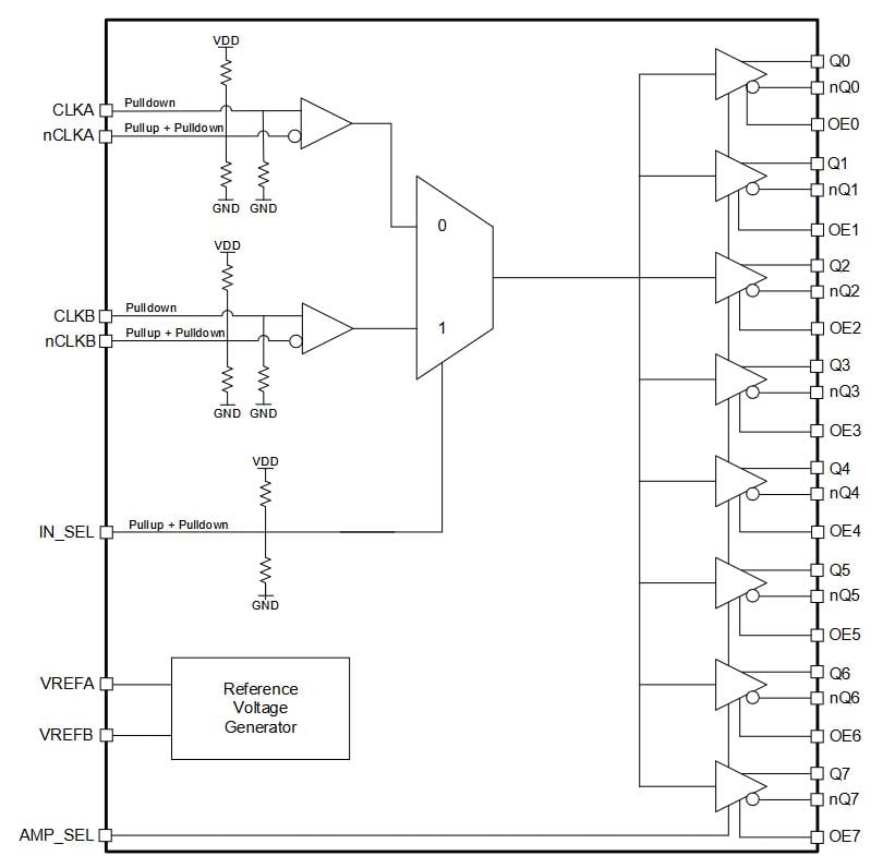
Two selectable differential inputs and eight low skew outputs are available. The integrated bias voltage reference enables easy interfacing of single-ended signals to the device inputs. The device is optimized for low power consumption and low additive phase noise.
The 8P34S1208-1 has an individual OE control pin for each output, which provides excellent control over the output enable functions.