

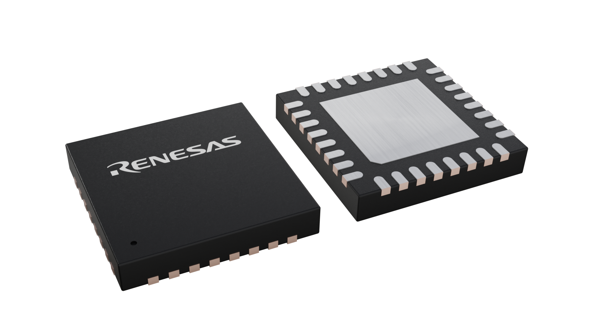

| CAD Model: | View CAD Model |
| Pkg. Type: | VFQFPN |
| Pkg. Code: | NLG32 |
| Lead Count (#): | 32 |
| Pkg. Dimensions (mm): | 5.0 x 5.0 x 0.9 |
| Pitch (mm): | 0.5 |
| Pb (Lead) Free | Yes |
| Moisture Sensitivity Level (MSL) | 3 |
| ECCN (US) | |
| HTS (US) |
| Pkg. Type | VFQFPN |
| Lead Count (#) | 32 |
| Pb (Lead) Free | Yes |
| Carrier Type | Tray |
| Advanced Features | Spread Spectrum |
| App Jitter Compliance | PCIe Gen1, PCIe Gen2, PCIe Gen3 |
| C-C Jitter Max P-P (ps) | 20 |
| Core Voltage (V) | 3.3 |
| Feedback Input | No |
| Input Freq (MHz) | 25100 - 25100 |
| Input Type | Crystal, HCSL, LVDS, LVHSTL, LVPECL |
| Inputs (#) | 2 |
| Length (mm) | 5 |
| MOQ | 490 |
| Moisture Sensitivity Level (MSL) | 3 |
| Output Banks (#) | 2 |
| Output Freq Range (MHz) | 100 - 500 |
| Output Skew (ps) | 85 |
| Output Type | HCSL |
| Output Voltage (V) | 3.3 |
| Outputs (#) | 4 |
| Package Area (mm²) | 25 |
| Pb Free Category | e3 Sn |
| Phase Jitter Typ RMS (ps) | 0.608 |
| Pitch (mm) | 0.5 |
| Pkg. Dimensions (mm) | 5.0 x 5.0 x 0.9 |
| Prog. Clock | No |
| Qty. per Carrier (#) | 490 |
| Qty. per Reel (#) | 0 |
| Reference Output | No |
| Requires Terms and Conditions | Does not require acceptance of Terms and Conditions |
| Spread Spectrum | Yes |
| Tape & Reel | No |
| Temp. Range (°C) | 0 to 70°C |
| Thickness (mm) | 0.9 |
| Width (mm) | 5 |
IDT's PLL-based clock generators offer sub-picosecond jitter, low-skew clock outputs, and edge rates that meet the ever-growing demands of today's networking solutions. The 871S1022 is a PLL-based clock generator specifically designed for PCI Express® Clock Generation applications. The device generates 100MHz, 125MHz, 250MHz or 500MHz from either a 25MHz fundamental mode crystal or a 100MHz recovered clock. The 871S1022 has two modes of operation: (1) high frequency jitter attenuator and (2) high performance clock synthesizer mode. When in jitter attenuator mode, the 871S1022 is able to both suppress high frequency noise components and function as a frequency translator. Designed to receive a jittery and noisy clock from an external source, the 871S1022 uses FemtoClock® technology to clean up the incoming clock and translate the frequency to one of the four common PCI Express® frequencies. When in synthesizer mode, the device is able to generate high performance SSC and non-SSC clocks from a low cost external, 25MHz, fundamental mode crystal. The 871S1022 uses FemtoClock® technology to generate low noise clock outputs capable of providing the seed frequencies for the common PCI Express® link rates.