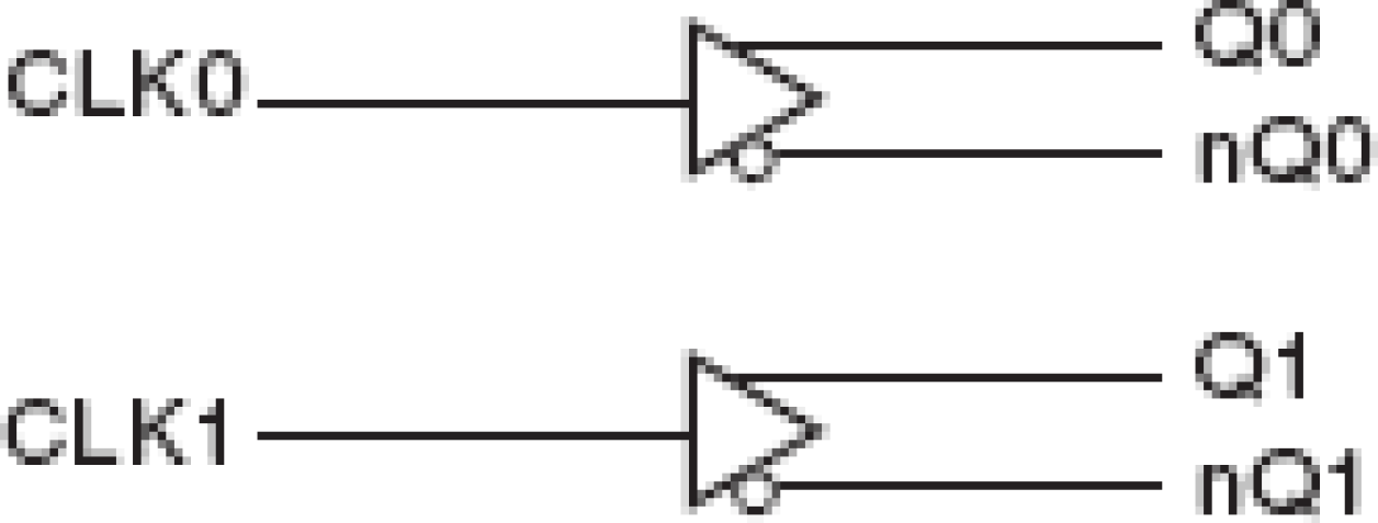
Package Information
| CAD Model: | View CAD Model |
| Pkg. Type: | SOIC |
| Pkg. Code: | DCG8 |
| Lead Count (#): | 8 |
| Pkg. Dimensions (mm): | 4.9 x 3.9 x 1.5 |
| Pitch (mm): | 1.27 |
Environmental & Export Classifications
| Moisture Sensitivity Level (MSL) | 1 |
| Pb (Lead) Free | Yes |
| ECCN (US) | EAR99 |
| HTS (US) | 8542.39.0090 |
Product Attributes
| Lead Count (#) | 8 |
| Carrier Type | Tube |
| Moisture Sensitivity Level (MSL) | 1 |
| Qty. per Reel (#) | 0 |
| Qty. per Carrier (#) | 97 |
| Pb (Lead) Free | Yes |
| Pb Free Category | e3 Sn |
| Temp. Range (°C) | 0 to 70°C |
| Core Voltage (V) | 2.5V, 3.3V |
| Function | Buffer |
| Input Freq (MHz) | 350 |
| Input Type | LVCMOS |
| Inputs (#) | 2 |
| Length (mm) | 4.9 |
| MOQ | 97 |
| Output Banks (#) | 2 |
| Output Freq Range (MHz) | 350 |
| Output Type | HSTL |
| Output Voltage (V) | 2.5V, 3.3V |
| Outputs (#) | 2 |
| Package Area (mm²) | 19.1 |
| Pitch (mm) | 1.27 |
| Pkg. Dimensions (mm) | 4.9 x 3.9 x 1.5 |
| Pkg. Type | SOIC |
| Product Category | Clock Buffers & Drivers |
| Requires Terms and Conditions | Does not require acceptance of Terms and Conditions |
| Tape & Reel | No |
| Thickness (mm) | 1.5 |
| Width (mm) | 3.9 |
Resources for 85222
Description
The 85222 is a Dual LVCMOS / LVTTL-to- Differential LVHSTL Translator. The 85222 has two single ended clock inputs. The single ended clock input accepts LVCMOS or LVTTL input levels and translates them to LVHSTL levels. The small outline 8-pin SOIC package makes this device ideal for applications where space, high performance and low power are important. For optimum performance, both output pairs need to be terminated, even if one output pair is unused.


