
| CAD Model: | View CAD Model |
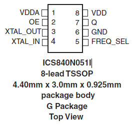
| Pkg. Type: | TSSOP |
| Pkg. Code: | PGG8 |
| Lead Count (#): | 8 |
| Pkg. Dimensions (mm): | 3.1 x 4.4 x 1.0 |
| Pitch (mm): | 0.65 |
| Moisture Sensitivity Level (MSL) | 1 |
| Pb (Lead) Free | Yes |
| ECCN (US) | EAR99 |
| HTS (US) | 8542.39.0090 |
| Lead Count (#) | 8 |
| Carrier Type | Reel |
| Moisture Sensitivity Level (MSL) | 1 |
| Qty. per Reel (#) | 2500 |
| Qty. per Carrier (#) | 0 |
| Pb (Lead) Free | Yes |
| Pb Free Category | e3 Sn |
| Temp. Range (°C) | -40 to 85°C |
| Core Voltage (V) | 2.5V, 3.3V |
| Feedback Input | No |
| Input Freq (MHz) | 19.2 - 19.2, 19.44 - 19.44, 19.5312 - 19.5312 |
| Input Type | Crystal |
| Inputs (#) | 1 |
| Length (mm) | 3.1 |
| MOQ | 2500 |
| Output Banks (#) | 1 |
| Output Freq Range (MHz) | 153.6 - 153.6, 155.52 - 155.52, 156.25 - 156.25, 76.8 - 76.8, 77.76 - 77.76 |
| Output Type | LVCMOS |
| Output Voltage (V) | 2.5V, 3.3V |
| Outputs (#) | 1 |
| Package Area (mm²) | 13.6 |
| Phase Jitter Max RMS (ps) | 0.138 |
| Phase Jitter Typ RMS (ps) | 0.101 |
| Pitch (mm) | 0.65 |
| Pkg. Dimensions (mm) | 3.1 x 4.4 x 1.0 |
| Pkg. Type | TSSOP |
| Product Category | FemtoClock, Ultra-Low Jitter Clocks (<300 fs RMS) |
| Prog. Clock | No |
| Reel Size (in) | 13 |
| Reference Output | No |
| Requires Terms and Conditions | Does not require acceptance of Terms and Conditions |
| Spread Spectrum | No |
| Tape & Reel | Yes |
| Thickness (mm) | 1 |
| Width (mm) | 4.4 |
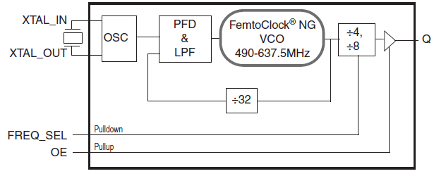
The 840N051I is a LVCMOS/LVTTL clock synthesizer designed for SDH/SONET and Ethernet applications. The device generates a selectable 156.25MHz or 77.76MHz clock signal with excellent phase jitter performance. It uses Renesas' fourth generation FemtoClock® NG technology for an optimum of high clock frequency, low phase noise performance and low power consumption. The device supports 2.5V or 3.3V voltage supply and is packaged in a small, lead-free (RoHS 6) 8-lead TSSOP package. The extended temperature range supports wireless infrastructure, telecommunication, and networking end equipment requirements.