

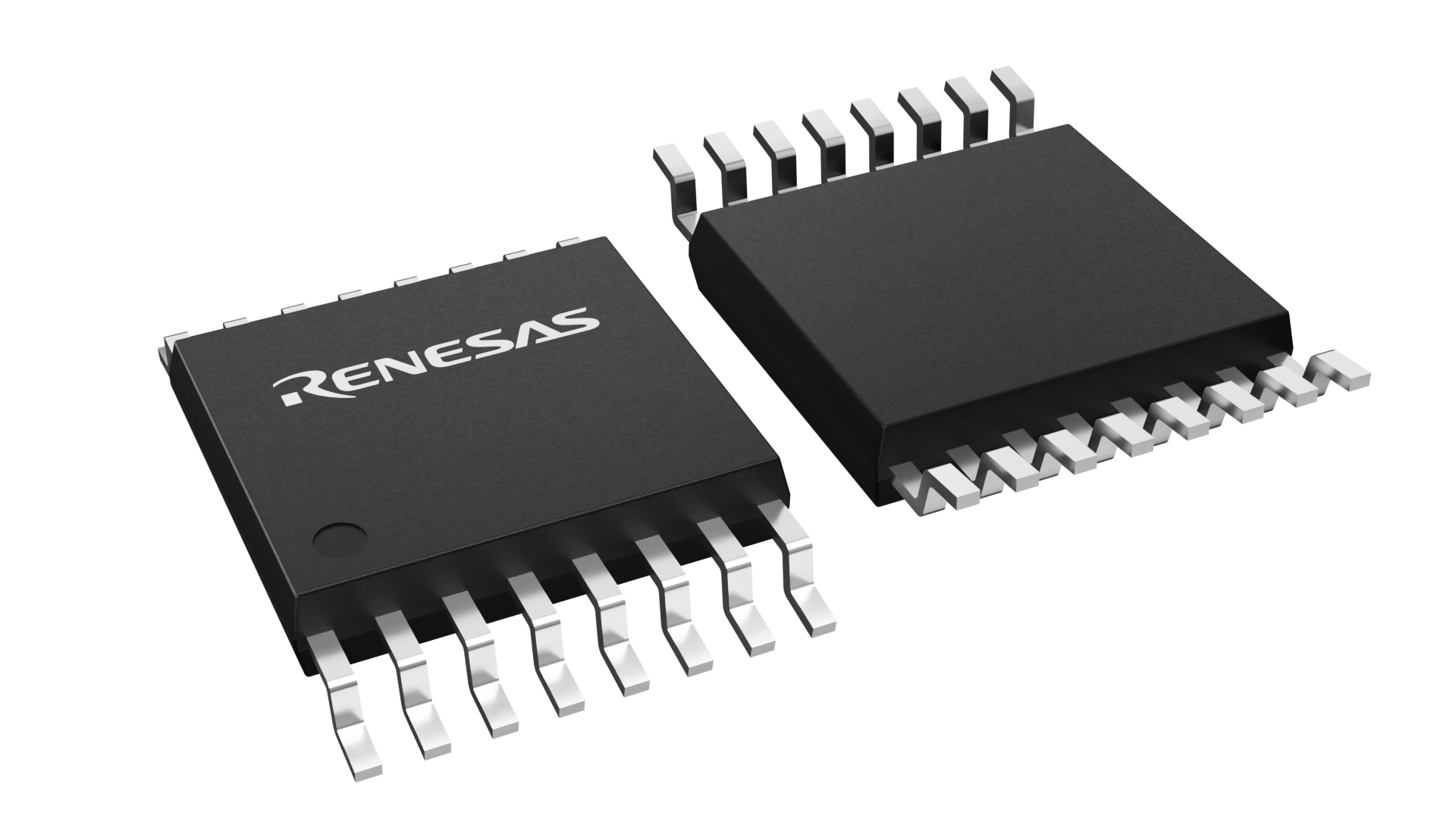

| CAD Model: | View CAD Model |
| Pkg. Type: | TSSOP |
| Pkg. Code: | PGG16 |
| Lead Count (#): | 16 |
| Pkg. Dimensions (mm): | 5.0 x 4.4 x 1.0 |
| Pitch (mm): | 0.65 |
| Moisture Sensitivity Level (MSL) | 1 |
| Pb (Lead) Free | Yes |
| ECCN (US) | EAR99 |
| HTS (US) | 8542.39.0090 |
| Lead Count (#) | 16 |
| Carrier Type | Tube |
| Moisture Sensitivity Level (MSL) | 1 |
| Qty. per Reel (#) | 0 |
| Qty. per Carrier (#) | 96 |
| Pb (Lead) Free | Yes |
| Pb Free Category | e3 Sn |
| Temp. Range (°C) | -40 to 85°C |
| Additive Phase Jitter Typ RMS (fs) | 140 |
| Additive Phase Jitter Typ RMS (ps) | 0.14 |
| Core Voltage (V) | 2.5V, 3.3V |
| Function | Multiplexer |
| Input Freq (MHz) | 250 |
| Input Type | LVCMOS |
| Inputs (#) | 4 |
| Length (mm) | 5 |
| MOQ | 192 |
| Output Banks (#) | 1 |
| Output Freq Range (MHz) | 250 |
| Output Type | LVCMOS |
| Output Voltage (V) | 1.8V, 2.5V, 3.3V |
| Outputs (#) | 1 |
| Package Area (mm²) | 22 |
| Pitch (mm) | 0.65 |
| Pkg. Dimensions (mm) | 5.0 x 4.4 x 1.0 |
| Pkg. Type | TSSOP |
| Product Category | Clock Multiplexers |
| Requires Terms and Conditions | Does not require acceptance of Terms and Conditions |
| Tape & Reel | No |
| Thickness (mm) | 1 |
| Width (mm) | 4.4 |
The 83054I is a low skew, 4:1, Single-ended Multiplexer and a member of the family of High Performance Clock Solutions from IDT. The 83054I has four selectable single-ended clock inputs and one single-ended clock output. The output has a VDDO pin which may be set at 3.3V, 2.5V, or 1.8V, making the device ideal for use in voltage translation applications. An output enable pin places the output in a high impedance state which may be useful for testing or debug purposes. The device operates up to 250MHz and is packaged in a 16 TSSOP package.