
| CAD Model: | View CAD Model |
| Pkg. Type: | COL |
| Pkg. Code: | CMG16 |
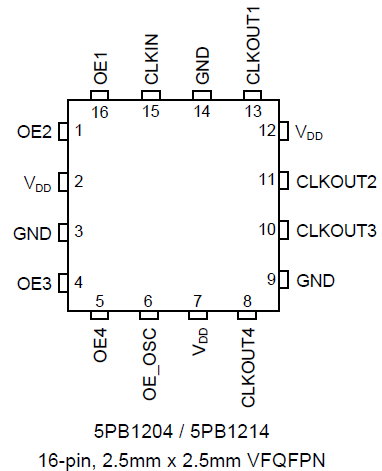
| Lead Count (#): | 16 |
| Pkg. Dimensions (mm): | 2.5 x 2.5 x 0.5 |
| Pitch (mm): | 0.4 |
| Moisture Sensitivity Level (MSL) | 1 |
| Pb (Lead) Free | Yes |
| ECCN (US) | EAR99 |
| HTS (US) | 8542.39.0090 |
| Lead Count (#) | 16 |
| Carrier Type | Reel |
| Moisture Sensitivity Level (MSL) | 1 |
| Pb (Lead) Free | Yes |
| Pb Free Category | e3 Sn |
| Temp. Range (°C) | -40 to 105°C |
| Country of Assembly | MALAYSIA |
| Country of Wafer Fabrication | TAIWAN |
| Additive Phase Jitter Typ RMS (fs) | 50 |
| Core Voltage (V) | 1.8 |
| Family Name | 5PB |
| Function | Buffer |
| Input Freq (MHz) | 200 |
| Input Type | LVCMOS, Sine Wave |
| Inputs (#) | 1 |
| Length (mm) | 2.5 |
| MOQ | 4000 |
| Output Banks (#) | 1 |
| Output Freq Range (MHz) | 200 |
| Output Signaling | LVCMOS |
| Output Skew (ps) | 65 |
| Output Type | LVCMOS |
| Output Voltage (V) | 1.8 |
| Outputs (#) | 4 |
| Package Area (mm²) | 6.3 |
| Pitch (mm) | 0.4 |
| Pkg. Dimensions (mm) | 2.5 x 2.5 x 0.5 |
| Pkg. Type | COL |
| Price (USD) | $1.22918 |
| Published | No |
| Qty. per Carrier (#) | 0 |
| Qty. per Reel (#) | 4000 |
| Reel Size (in) | 7 |
| Reference Output | Yes |
| Requires Terms and Conditions | Does not require acceptance of Terms and Conditions |
| Spread Spectrum | No |
| Tape & Reel | Yes |
| Thickness (mm) | 0.5 |
| Width (mm) | 2.5 |
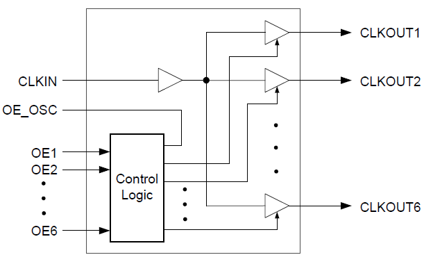
The 5PB1204 is a high-performance TCXO/LVCMOS clock fanout buffer with individual OE pins for each output. The CLKIN pin can accept either a square wave (LVCMOS) or a clipped sine wave (such as TCXO clipped sine wave output) as input.
The 5PB1204 has industry-leading low jitter and extremely low current consumption, making it ideal for smart mobile devices.