
| CAD Model: | View CAD Model |
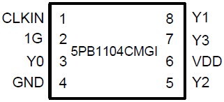
| Pkg. Type: | TSSOP |
| Pkg. Code: | PGG8 |
| Lead Count (#): | 8 |
| Pkg. Dimensions (mm): | 3.1 x 4.4 x 1.0 |
| Pitch (mm): | 0.65 |
| Moisture Sensitivity Level (MSL) | 1 |
| Pb (Lead) Free | Yes |
| ECCN (US) | EAR99 |
| HTS (US) | 8542.39.0090 |
| Lead Count (#) | 8 |
| Carrier Type | Tube |
| Moisture Sensitivity Level (MSL) | 1 |
| Qty. per Reel (#) | 0 |
| Pkg. Dimensions (mm) | 3.1 x 4.4 x 1.0 |
| Package Area (mm²) | 13.6 |
| Pitch (mm) | 0.65 |
| Qty. per Carrier (#) | 96 |
| Pb (Lead) Free | Yes |
| Pb Free Category | e3 Sn |
| Temp. Range (°C) | -40 to 85°C |
| Country of Assembly | TAIWAN |
| Country of Wafer Fabrication | CHINA, TAIWAN |
| Additive Phase Jitter Typ RMS (fs) | 35 |
| Core Voltage (V) | 1.8V, 2.5V, 3.3V |
| Family Name | 5PB |
| Function | Buffer |
| Input Freq (MHz) | 200 |
| Input Type | LVCMOS |
| Inputs (#) | 1 |
| Length (mm) | 3.1 |
| Longevity | 2040 Apr |
| MOQ | 288 |
| Output Banks (#) | 1 |
| Output Freq Range (MHz) | 200 |
| Output Skew (ps) | 65 |
| Output Type | LVCMOS |
| Output Voltage (V) | 1.8V, 2.5V, 3.3V |
| Outputs (#) | 4 |
| Pkg. Type | TSSOP |
| Price (USD) | $1.25939 |
| Published | No |
| Requires Terms and Conditions | Does not require acceptance of Terms and Conditions |
| Tape & Reel | No |
| Thickness (mm) | 1 |
| Width (mm) | 4.4 |
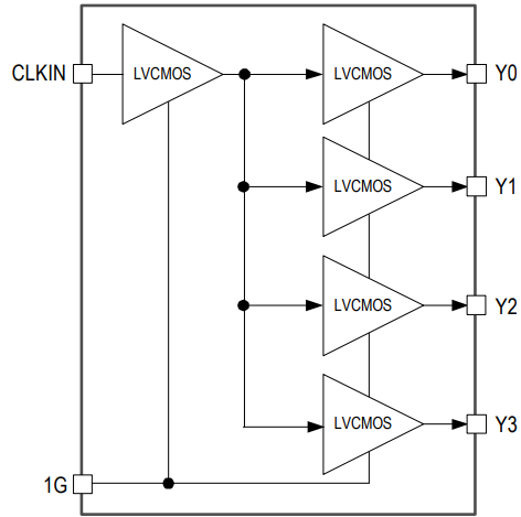
The 5PB1104 is a high-performance 1:4 LVCMOS clock buffer that offers a best-in-class additive phase jitter of 50fs RMS. This clock buffer also supports an Output Enable function. It is available in 8-pin DFN and TSSOP packages and can operate from a 1.8V to 3.3V supply.