

| CAD Model: | View CAD Model |
| Pkg. Type: | LGA |
| Pkg. Code: | LTG24 |
| Lead Count (#): | 24 |
| Pkg. Dimensions (mm): | 4.0 x 4.0 x 1.4 |
| Pitch (mm): | 0.5 |
| Moisture Sensitivity Level (MSL) | 3 |
| Pb (Lead) Free | Yes |
| ECCN (US) | EAR99 |
| HTS (US) | 8542.39.0090 |
| Lead Count (#) | 24 |
| Carrier Type | Tray |
| Moisture Sensitivity Level (MSL) | 3 |
| Qty. per Reel (#) | 0 |
| Qty. per Carrier (#) | 490 |
| Pb (Lead) Free | Yes |
| Pb Free Category | e4 Au |
| Temp. Range (°C) | -40 to 85°C |
| Country of Assembly | TAIWAN |
| Country of Wafer Fabrication | SINGAPORE |
| Advanced Features | Programmable Clock, Reference Output, Spread Spectrum |
| App Jitter Compliance | PCIe Gen1, PCIe Gen2, PCIe Gen3, PCIe Gen4, PCIe Gen5 |
| Architecture | Common, SRNS, SRIS |
| C-C Jitter Typ P-P (ps) | 46 |
| Core Voltage (V) | 1.8V, 2.5V, 3.3V |
| Diff. Output Signaling | HCSL, LVDS, LVPECL, LVCMOS |
| Diff. Outputs | 4 |
| Family Name | VersaClock 6E |
| Function | Generator |
| Input Freq (MHz) | 1 - 350 |
| Input Type | Crystal, LVCMOS, LVPECL, LVDS, HCSL |
| Inputs (#) | 1 |
| Length (mm) | 4 |
| Longevity | 2040 Apr |
| MOQ | 490 |
| NXP Processor Function | Memory Clock, SerDes Clock, CPU/USB/Eth Clock |
| Output Banks (#) | 4 |
| Output Freq Range (MHz) | 1 - 350 |
| Output Impedance | 100 |
| Output Skew (ps) | 75 |
| Output Type | LVCMOS, LVPECL, HCSL, LVDS |
| Output Voltage (V) | 1.8V, 2.5V, 3.3V |
| Outputs (#) | 5 |
| Package Area (mm²) | 16 |
| Phase Jitter Typ RMS (fs) | 500 |
| Phase Jitter Typ RMS (ps) | 0.5 |
| Pitch (mm) | 0.5 |
| Pkg. Dimensions (mm) | 4.0 x 4.0 x 1.4 |
| Pkg. Type | LGA |
| Power Consumption Typ (mW) | 100 |
| Price (USD) | $4.16415 |
| Prog. Clock | Yes |
| Prog. Interface | I2C, OTP |
| Published | No |
| Reference Output | Yes |
| Spread Spectrum | Yes |
| Supply Voltage (V) | 1.8 - 1.8, 2.5 - 2.5, 3.3 - 3.3 |
| Tape & Reel | No |
| Thickness (mm) | 1.4 |
| Width (mm) | 4 |
| Xtal Freq (MHz) | 8 - 40 |
| Xtal Inputs (#) | 1 |
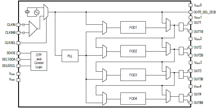
The 5P49V6975 is a member of Renesas' VersaClock® 6E programmable clock generator family. The 5P49V6975 is intended for high-performance consumer, networking, industrial, computing, and data-communications applications. The reference clock can come from one of the two redundant clock inputs. A glitchless manual switchover function allows one of the redundant clocks to be selected during normal operation.
Configurations may be stored in on-chip One-Time Programmable (OTP) memory or changed using I²C& interface.